OPPO UDP-203 4K
OPPO UDP-205 4K
OPPO PM-1
OPPO PM-2
OPPO PM-3
OPPO HA-2SE
Sonica DAC
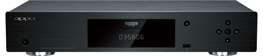
OPPO UDP-203 4K
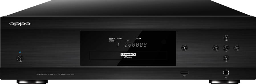
OPPO UDP-205 4K

OPPO PM-1
OPPO PM-2
OPPO PM-3
OPPO HA-2SE
Sonica DAC
Understanding the HDMI Audio Jitter Reduction Circuit in the OPPO UDP-205
The Challenge
HDMI is the most commonly used audio/video interface these days, delivering ultra-high definition video and high resolution audio from source devices like Blu-ray Disc players to downstream equipment such as TVs and A/V processors or receivers. While HDMI has been great for transmitting video with its huge bandwidth, audio enthusiasts often question its ability to carry audio. Transmitting digital audio requires two elements: audio data and clock. The question is not about whether HDMI can carry digital audio data accurately in a bit-for-bit perfect sense (it can!), but whether it can deliver the data bits at perfect time intervals based on the original audio clock timing. When data bits arrive at slightly varying time intervals, the problem is called "jitter" and it has negative impact on the quality of converting the audio data back to audible sound, a process called digital-to-analogue conversion.
The problem of digital audio jitter has been well documented and thoroughly discussed by industry experts, for a brief overview, the About Jitter: Digital Audio's Weakest Link presentation by the experts at ESS Technology is a good reference.
The HDMI technology was developed from DVI (Digital Video Interface), which does not carry audio at all. When the requirement to carry audio appeared for HDMI, the decision was made that audio data should be carried in data packets and inserted into so called "data islands" during the blanking interval of video. This way no extra wire or bandwidth is needed in order to carry audio, and the audio clock signal is completely eliminated over HDMI. Instead, HDMI defines a mechanism to reconstruct the audio clock on the receiving side using the video clock and a pair of multiplier and divisor values called N and CTS.
At the receiving side, the audio clock is reconstructed from the video clock using a clock divider and a clock multiplier following this formula:
128*fs = fv * N / CTS
"fs" is the audio clock frequency. "fv" is the video clock frequency. "N" is a constant defined by the HDMI specification. "CTS" is called a Cycle Time Stamp because it is generated by counting the number of video clock pulses in each of the 128*fs/N time frame. The HDMI cable has a dedicated pair of wires for carrying the video clock. N and CTS values are transmitted to the receiving side using special "Audio Clock Regeneration Packets" so that the receiving side has all three parts to reconstruct the audio clock.
For example, when sending an audio signal with a 44.1 kHz sample rate with a 1080p 60 Hz video signal, the video clock is 148.5 MHz, N is 6272, and CTS is 165000. The hardware on the receiving side can reconstruct a 44.1 kHz clock signal by doing this simple maths:
((148,500,000 * 6272) / 165,000) / 128 = 44,100
The above example is the ideal scenario, but in a real piece of consumer electronics equipment, the situation is not that simple.
Now consider that the video clock may not be exactly 148.5 MHz (CEA and VESA standards allow a +/- 0.5% video clock frequency tolerance), and that the video clock may have high jitter (HDMI 1.4 specifications allow a 0.25 Tbit [25% of a clock cycle time] clock jitter at the transmitting end), the quality of the reconstructed audio clock can definitely be affected by the quality of the video clock.
Another potential problem is that at the source side, the video clock frequency is decided by the video format used, while the audio clock frequency is usually a fixed value based on the original audio encoding. The video and audio clocks may not originate from a common clock source, so it might not be possible to get a fixed CTS value. For example, if the audio clock is 32 kHz and the video is 720p 59.94 Hz, the CTS value would be alternating between 210,937 and 210,938 because there is no rational (integer divided by integer) relationship between the two clock frequencies. When the CTS value keeps changing, the reconstructed audio clock will have higher jitter.
The Solution
In the OPPO UDP-205 Audiophile UHD 4K Blu-ray Disc player, OPPO engineers address the two problems outlined above with a unique HDMI Audio Jitter Reduction Circuit. The goal of this circuit is to provide a very stable video clock and a constant integer CTS value. This way when the receiving side reconstructs the audio clock, it has a clock source with extremely low jitter to begin with, and there is no extra jitter induced by a varying CTS value.
The main challenge for getting a very stable video clock in a universal disc player is the many video formats that must be supported. Different video formats require different video clock frequencies. It is not possible to generate all of these frequencies directly from many clock oscillators, so instead a master clock and multiple PLLs (Phase Locked Loops) are used to generate the required video clock frequencies. However the use of multiple PLLs degrades the quality of the video clock in comparison to the original master clock. Fortunately, the UDP-205 has two HDMI ports: an HDMI 2.0 port supporting all video formats including Ultra HD, and an audio-only HDMI port. Since the actual video can be carried over the main HDMI 2.0 port, OPPO engineers can completely discard the original video clock on the audio-only HDMI port, and replace it with a dedicated high stability and ultra-low jitter master clock.
What is the best frequency for this new master clock? OPPO engineers looked deep into the HDMI specifications and decided on the 148.5 MHz frequency. This 148.5 MHz is a magic number. It is the video clock frequency for the 1080p 50 Hz and 1080p 60 Hz video formats, the two highest formats supported by HDMI 1.4. Since audio bandwidth over HDMI is directly dependent on the video bandwidth, having the highest video bandwidth ensures that the UDP-205 can handle all high-resolution audio formats. The 148.5 MHz video clock frequency also has a rational relationship with all common audio clock frequencies, resulting in constant CTS values for all sample rates including 32 kHz, 44.1 kHz, 88.2 kHz, 176.4 kHz, 48 kHz, 96 kHz, 192 kHz, and so on. The following table summarises the N and CTS values using this 148.5 MHz clock for all these audio sample rates:
| Audio Sample Rate | N value | CTS value |
| 32 kHz | 4096 | 148500 |
| 44.1 kHz | 6272 | 165000 |
| 88.2 kHz | 12544 | 165000 |
| 176.4 kHz | 25088 | 165000 |
| 48 kHz | 6144 | 148500 |
| 96 kHz | 12288 | 148500 |
| 192 kHz | 24576 | 148500 |
OPPO engineers set out to look for the best 148.5 MHz clock source for this design, and ended up having Seiko Epson Corporation custom-build a Surface Acoustic Wave (SAW) oscillator for the UDP-205. When compared to crystal oscillators (XO) or crystal oscillators with PLLs (PLL-XO), a SAW oscillator has significant advantages. SAW is able to produce high frequencies with fundamental mode oscillation only, resulting in a clean clock source with no spurs and does not exhibit frequency jumps. It does not require PLLs to achieve the 148.5 MHz output. SAW has ultra-low jitter and excellent phase noise performance. The long term stability and reliability of SAW are far better than a crystal oscillator at the same 148.5 MHz frequency since the crystal tuning fork will be too thin to be reliable. The SAW oscillator clock source ensures that the UDP-205 has the best possible clock signal for HDMI audio.
In order to further remove the dependency of the audio signal to video, the UDP-205 utilises a special video pattern generator chip to create a video stream with full black content and sends the black video with the high quality clock to the downstream audio processor or receiver.
Once the signal reaches the receiving end, for PCM and DSD audio, the reconstructed audio clock is usually used directly to drive the audio data. As a result, the HDMI audio jitter reduction circuit can improve the sound quality of PCM and DSD audio directly. For bitstream audio in compressed formats such as Dolby Atmos, Dolby TrueHD, DTS:X or DTS-HD Master, the jitter reduction benefit depends on whether the decoder design in the audio processor/receiver uses a synchronous or asynchronous clock. Compressed audio decoding requires buffering of the audio data and performing mathematic manipulations. If the decoder uses a synchronous clock design, the decoded data is usually driven out with a clock that is 1x, 2x, or 4x that of the reconstructed audio clock but synchronised to it, so the benefit can carry over. If the decoder uses a completely new, locally generated clock to drive out the decoded data, then jitter reduction on the player side is not a benefit, but the same circuit ensures error-free delivery of the bitstream audio data to the decoder thanks to a very stable HDMI video clock and a constant CTS value.
The Results
So how does the HDMI audio jitter reduction circuit of the OPPO UDP-205 perform? OPPO engineers conducted lab tests to find out and here are the results.
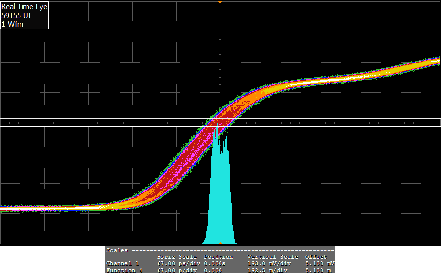
First, take a look at the HDMI video clock quality. Since the clock frequency is very high, jitter measurements at this frequency must be done with special test equipment that captures an "Eye Diagram".
This is the zoomed-in eye diagram of the normal 1080p video clock from the UDP-205. The clock jitter is measured to be 0.080 Tbit, or 53.82 ps.
This is the zoomed-in eye diagram of the video clock after the HDMI jitter reduction circuit is inserted. The clock jitter is measured to be 0.075 Tbit, or 50.67 ps.
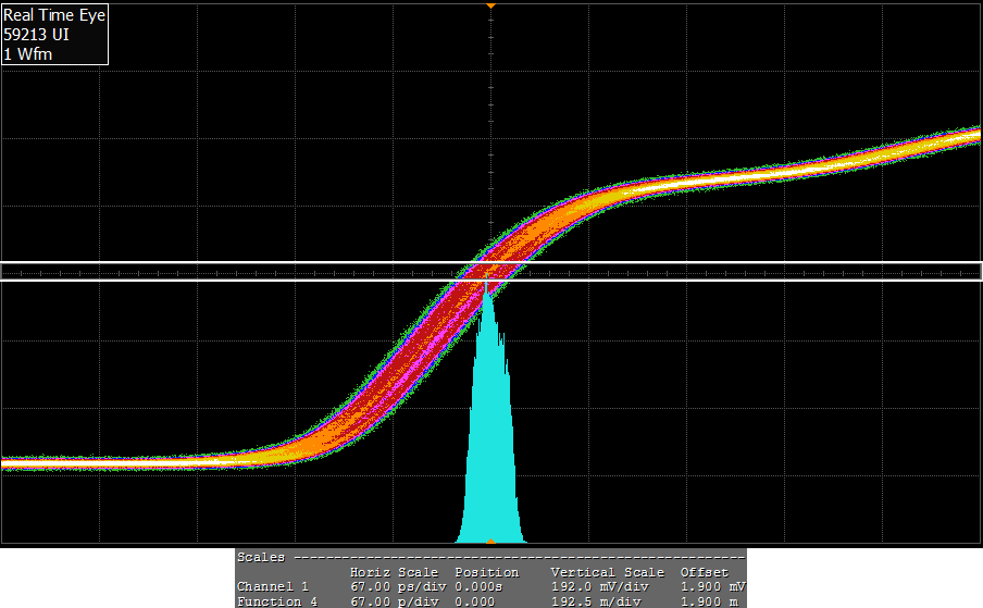
As can be seen from the above eye diagrams and measurements, the HDMI clock jitter has been reduced. Although the reduction is only a few pico-seconds and does not seem to be a big percentage, keep in mind that the UDP-205 is already a very high performance design to begin with, and any small performance gain is like a cherry on top.
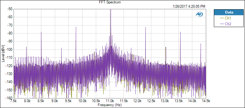
Next, OPPO engineers used the famous "J-test" audio signal to test the actual impact to digital audio transmission over HDMI. The player plays the J-test audio file, which is a high level main signal at 1/4 the sample rate with a low level square wave modulation at 1/192 of the sample rate. The digital audio signal is transmitted over HDMI, and then converted to analogue audio by an A/V processor. The analogue signal is then processed by FFT (Fast Fourier Transform) to show the energy of all frequencies around the original high level signal. Jitter artifacts are shown as sidebands around the main signal. The higher the sideband levels are, the higher the jitter is.
In order to isolate the benefit of the UDP-205’s HDMI jitter reduction circuit, the engineers intentionally selected a lower end mass market A/V processor for this experiment. The reason is that some high-end A/V processors have their own clock regeneration or clock isolation circuit, so the test result may be attributed to the A/V processor’s design rather than the UDP-205. Using a mass market A/V processor may not reveal the best possible performance from the UDP-205, but the key here is to identify the sidebands to see how the jitter reduction circuit performs.
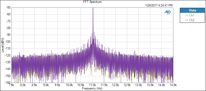
This image below is the zoomed-in FFT of the J-test signal transmitted by a prototype UDP-205 using the original 1080p video clock. Note that the two high sidebands are at around the -100 dB level.
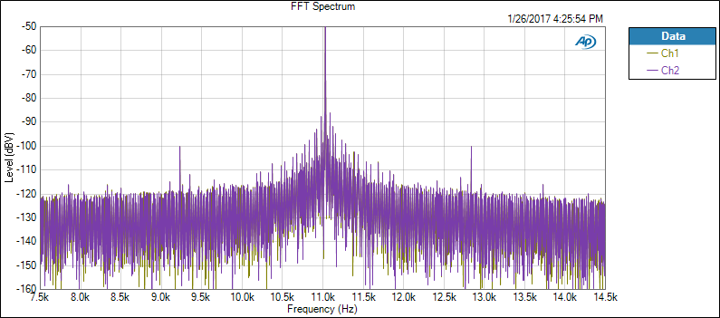
The next image is the zoomed-in FFT of the J-test signal transmitted by the same UDP-205 using the special 148.5 MHz HDMI clock. Note the sideband level is reduced to about -115 dB. This is a significant reduction of actual audio jitter artifacts.
Just for the sake of comparison, the following is the same J-test signal played via a competitor’s Blu-ray Disc player, whose brand and model will remain unidentified.
The Conclusion
The HDMI jitter reduction circuit in the UDP-205 is a unique design which can significantly reduce jitter and eliminate timing errors. Customers can enjoy their music with increased accuracy when using the audio-only HDMI output port for connecting the audio signal to an A/V processor or receiver.
News and events| Contact us| Where to buy|
Customer Service Hours : Mon- Fri. 9:30 AM- 5:30 PM (CET)  +49 341 4783 9885
© OPPO 2018 All rights reserved